Awesome. For those considering exploring some of these steps in their own garage -- the chemistry is dangerous, perhaps HF in particular, as it doesn't hurt, it just kills you a few hours later.
Can you do this in a garage? Absolutely, but learn everything you need to know from an ensemble of safety-minded mentors before you strike out on your own.
It's not just about safety for you, proper disposal of these chemicals is essential for the many generations to come. Sometimes it is inexpensive, sometimes it is costly. You need to know how before you start, or it costs a lot more.
(Also, you can get someone else to pay for the hardware, the infrastructure, the material, the resists, the reagents, the safety training, and the waste disposal if you work/volunteer at a university's photolithography facility. They'll probably pay you, too.)
I needed to dissolve(ha!) fluorite once. You can get it started by adding a few drops of conc H2SO4 to your beautiful aqua regia solution. It goes deeper red, some happy bubbles appear, and as long as it stays put, makes it's own "aqua nasty"(pg88) as you gently add your powdered sample.
I thought AQR+SA was called aqua nasty, but I cant get any hits other than this AA pdf with explicit HF added. Maybe an actual chemist can chime in, is there another name for the aqua regia +H2SO4 mix?
If I remember correctly in the book: "1636: The Chronicles of Dr. Gribbleflotz" he made "aqua regia" from "aqua fortis" and "acidum salis" I don't know if either of those were his name for aqua-regia + HydroSulphuric Acid. I know he called ethanol "aqua vitae" by repeatedly distilling wine. He also had "Oil of Vitriol" which he added to saltpeter to make "aqua fortis". He also talked about adding "Oil of Vitriol" to "aqua fortis" but doesn't say what it makes. I think maybe "oil of vitriol" was hydro sulfuric acid, but I am not sure. Perhaps you can find more or someone else can remember. (I used: https://www.ericflint.net/index.php/2016/06/03/1636-the-chro... to quote what I mentioned here.)
Aqua regia is just the name for a mixture of nitric and hydrochloric acid which has the ability to dissolve gold. Aqua fortis was simply an archaic name for nitric acid; acidum salis (literally "salt acid") is likewise an old alchemical name for hydrochloric acid, rather straightforwardly named because it was an acid that was synthesized from salt. (If you ever see hydrochloric acid referred to as "muriatic acid", this is just a somewhat more modernized version of the same name: brine-y/salty acid.)
Oil of vitriol is sulfuric acid. This was also quite a logical name at the time - it's an oily liquid that was made from vitriol (a common term for a class of brightly colored metal sulfate crystals).
So, in the reaction given, when the sulfuric acid is added to saltpeter (potassium nitrate), the sulfate ion swaps places with the nitrate ion and you instead get nitric acid and potassium sulfate.
Source: Have spent far, far too much time researching alchemical nomenclature because I thought it was cool.
Not really. Rectal administration of drugs is one of the fastest ways to administer a drug outside of IV.
Unfortunately, I found out about it because of a now-deceased friend who succumbed to alcoholism. Near the end, he would drink rectally, since his esophagus was effectively destroyed. Also, since there's no gag reflex to keep you safe, this way is one of the easiest ways to kill yourself with alcohol.
    INHALATION

    Estimates of the lowest lethal concentrations for hydrogen fluoride range from 50-250 ppm for 5-minute exposure and are based on accidental, ***voluntary*** and occupational exposure information.
>> For those considering exploring some of these steps in their own garage -- the chemistry is dangerous, perhaps HF in particular, as it doesn't hurt, it just kills you a few hours later.
I was hoping that with 50 years of development behind us, the home fabricators could use less complex methods and less hazardous chemicals. In other words, can the folks who lived it help people like this by saying "If we had to do it over, I'd go about it like...."
Any suggestions? If you had to reboot the chip fab business on a budget what would be a more practical approach?
I used to work in a fab. As far as I know, there's no acceptable way to remove native oxide without HF. We do have another etch process -- dry etch -- that uses plasma instead, but it causes surface damage, and you don't want that under the gate. Also, dry etch chambers are a lot more work to maintain than a fume hood where you do wet etch. Furthermore, dry etch has its own set of hazards, and you have to deal with a lot more potentially toxic vapor.
Thinking a little more outside the box, you might look into using germanium instead of silicon. I don't know much about the germanium system, except that it supposedly grows less oxide. You're still going to have to deposit and remove oxide somehow, though, which means CVD reactors and silane. It's not going to be easy to get away from explosive toxic gases and dirty processes.
Not to mention DiBorane and Arsene... 1000C anneal cycles, teratogenic photoresist ethers, UHV equipment, and muti-kW RF sources. It's possible to demonstrate um scale MOS with a small lab, but not safely in anything resembling a normal garage. Hoping to replicate a multi-$B process at home is a fool's errand.
While we're at it, a modern scanner costs many million dollars, weighs tons, and sits on its own separate foundation on pilings that go down to bedrock so that it doesn't pick up vibrations from the air handling systems. DIY it ain't :)
A scanner is a photolithography tool like a stepper, except instead of exposing the entire shot at once, it sweeps (scans) a narrow rectangular exposure across the shot, and then steps to the next one. This allows for lighter, more precise optics. Confusingly, there's a piece of standard office equipment with the same name. Even more confusingly, Canon makes both kinds! Be sure you call the right technician for service.
I use "Armour Etch" to remove oxide from chips for reverse engineering, so it might work instead of HF for home chip fabrication. It contains bifluroride salts so it's somewhat safer (although I'm still very careful with it). You can buy it in craft stores for etching glass.
There's just...no reason at all to do it for business purposes. If you're a prepper or looking for a science project I can understand it, it's a cool project. But from a business perspective you can buy the same thing but better for dollars and have it the next day.
The lowest-cost options I know of for commercial custom chip fabrication are MOSIS and CMP. Their pricing starts at €650 for 0.35 μm, but it's true that the result is much better. However, turnaround time is measured in weeks. You seem to be suggesting that there are options that are one order of magnitude faster and two orders of magnitude cheaper (but perhaps with a much coarser feature size).
I'm here to second the recommendation to work, volunteer, or take a class at a university. I took a class on MEMS at my university, and for only a few hundred bucks got access to a fully stocked lab with proper training and supervision. It was a good experience I would recommend to anyone interested.
Citation needed? The inorganic materials used in semiconductor fabrication, especially in the early days, tend to be fairly benign and are used only in small quantities relative to other industry.
The HF monster everyone is talking about in this thread is dangerous only as a concentrated acid. It's highly soluble -- reduce it with a rainstorm or two and let it recombine to a neutral pH and you rapidly get to (literally!) toothpaste-level toxicity.
There's a VERY serious discussion to be had about the safety for a backyard chip fabricator. But the idea that this is some kind of long term pollutant (relative to much more serious issues like the cleaning solutions in your very own closet!) is pretty spun.
Edit: yeah, as the responses point out, the "superfund" sites in question are things like VOC contamination you see with any urban industry, nothing particular to semiconductor fabrication that would justify the upthread quote about contamination "for many generations to come".
“We were putting into industrial production a lot of really nasty chemicals. There was just no knowledge of these things, and we were pouring stuff down into the city sewer system.” - Gordon Moore
> So it was that while running, but not so much as to force my body into open rebellion, I noticed something odd. When I was heading down the gently sloping hill on Peter Coutts Road towards Stanford Avenue, I turned right as usual to head back home, passed along the edge of a grassy area, and smelled...cookies. But not really cookies. Raw cookie dough. Outside.
No citation is needed when a simple internet search reveals plenty of references, and that the issue is not HF specifically - volatile organics are an important issue.
And I would argue that individuals have the right to commence with research and creation. Science is not 'easy stuff that harms nobody'. The Curies suffered radiological poisoning but furthered chemistry and physics a great deal. I would think that "computer science" has mollified people in thinking that science is painless, harmless venture of fun exploration. Go read up about the countless physicists and chemists who tried to crack fluorine.
If you are a scientist, and not in a sciency-y setting (lab), have a laminated clipboard stating chemical threats, electrical threats, biogenic threats, and particulate threats.
You may end up killing yourself. If you do, you did so in the name of science. Please, don't have others die because you failed to properly notify first responders of a threat.
Thanks for saying this. I worked for a few years at a semiconductor fab r&d facility. (As a tenant) Seemingly everything associated with this stuff is toxic and polluting. The old timer war stories include stuff like accidental releases that stripped paint from all of the cars in the adjacent lot.
Nasty stuff — the wisdom promoting garage stuff like this is questionable. :)
Oh, yeah. I knew someone would get around to linking to Derek Lowe and his inimitable "Things I Won't Work With" series. His best-known entry in that series, about chlorine triflouride, also has mention of HF and semiconductors:
> The compound also a stronger oxidizing agent than oxygen itself, which also puts it into rare territory. That means that it can potentially go on to “burn” things that you would normally consider already burnt to hell and gone, and a practical consequence of that is that it’ll start roaring reactions with things like bricks and asbestos tile. It’s been used in the semiconductor industry to clean oxides off of surfaces, at which activity it no doubt excels.
> There’s a report from the early 1950s (in this PDF) of a one-ton spill of the stuff. It burned its way through a foot of concrete floor and chewed up another meter of sand and gravel beneath, completing a day that I’m sure no one involved ever forgot. That process, I should add, would necessarily have been accompanied by copious amounts of horribly toxic and corrosive by-products: it’s bad enough when your reagent ignites wet sand, but the clouds of hot hydrofluoric acid are your special door prize if you’re foolhardy enough to hang around and watch the fireworks
Here's a video of some French people introducing the substance to things like a rubber glove and leather:
TL;DR "hydrofluoric acid is a water solution of hydrogen fluoride, HF. That’s a gas, and it’s a lot worse. ... As soon as it hits anything moist – like your lungs – it dissolves in the water and turns into hydrofluoric acid again."
The fact that it is liquid at relatively balmy temperatures makes it a bit easier to handle than most gases, but then you better have great urethane seals, gloves and clothing everywhere. (Silicones are permeable, PTFE is damaged over time, nitrile and vinyl gloves also leak.)
The exhaust lines on high-energy implanters (the ones that do P doping) are a treat. They get coated up with deposits of solid phosphorus. If accidentally exposed to atmosphere, they do what phosphorus does. We used to call it "unscheduled exhaust system PM." Medium and high current implanters where I worked accumulated arsenic in the exhaust system, but at least that doesn't explode on you.
Even then, you can only work with it in teams of at least 2, all being certified to work with HF, only during normal business hours, and with a safety checklist a mile long, which includes checking to see that the calcium gluconate in the emergency kit is unopened and unexpired, and there are extra gloves with it, so the person applying it to you does not also get poisoned just by touching you.
That reminds me of why I decided against buying a portable sawmill. The nice ones come with an amputation kit, so when you cut something off accidentally there's a tourniquet on hand to slow the bleeding.
This comment is misinformed and should be deleted because it is so dangerous. HF will kill you for looking at it in the wrong way; please don't handle it unless you understand the danger it poses to you and the people around you.
Why is this comment misinformed? In a video tour of his home lab, Sam Zeloof shows us his acid-storage cabinet and mentions that he gets HF from over-the-counter Whink-brand "Rust Stain Remover"[1].
Since this product is commonly available at hardware stores across the United States, why should comments related to it "be deleted because it is so dangerous"?
I agree that HF can be extremely dangerous, but in this case it's not clear that Sam is working with or advocating use of dangerous concentrations or chemcial forumulations of fluorine-based acids. Maybe I missed a post where he does discuss using more dangerous concentrations or compounds?
I hope your "water gun" is made entirely of polypropylene, neoprene, polytetrafluoroethane, polyvinyl fluoride, wax, lead, and/or polyethylene.
And that you're wearing a chemical protection suit with respirator while playing with it. And that you are well aware of wind and weather conditions. And that you take care to keep it out of the environment.
Seems like one of those things that would be more dangerous to the wielder than anyone else.
His website and Youtube channel are so richly filled with knowledge that so desperately needs to be in the public domain, instead of being locked in corporate structures.
"His website and Youtube channel are so richly filled with knowledge that so desperately needs to be in the public domain, instead of being locked in corporate structures."
All of this information is public domain, what are you talking about? This is extremely well understood stuff.
Yeah, I went a bit overboard in my amazement that this exploration into building integrated circuitry with affordable tools was so well documented. Such practical information and experience is hard to come by in world where the manufacturing of integrated circuits has been iterated on with very expensive machinery for at least 50 years.
> I'm not sure if I should admire or condone this kind of attitude in a science related context.
It makes no difference whatsoever to the whole what you’ve pointed out here.
Throughout the video, she states she’s responding to critics. Her whole attitude is of teasing those who accuse her of not knowing what she does (calling her chips fake, etc).
When she says that, it’s perfectly clear that she’s being very (and I mean very) sarcastic.
We can discuss if her use of sarcasm is useful or not, but then we will be discussing the specifics of her presentation, not her skills at doing the chemical process she just demonstrated.
Since this is a video about “Making Microchips at Home”; since she’s responding to critics; I think we can allow her some room to throw some sarcasm to the mix, even if it does not work out completely as intended.
On a side note: it would be nice if people on the internet would allow others some “humanity"; by that meaning giving them room to err, like saying silly things when they are annoyed — instead of nitpicking bits of unimportant information.
Normally I would agree with you. But these days when anyone can find support for, as well as buy, almost anything on the Internet our freedom to be imprecise and still responsible has unfortunately diminished significantly. That of course doesn't justify a lot of other comments, or attitudes, people have to deal with when wanting to make something.
> our freedom to be imprecise and still responsible has unfortunately diminished significantly
I disagree. The responsibility has and should always remain entirely with the person taking the action. If speaking imprecisely on the Internet is a liability then nobody can speak at all.
Random YouTube maker videos have virtually zero duty of care to their audience.
I say virtually because I could imagine a maliciously crafted video designed to lull a watcher into inadvertently blowing themselves up, but even in the case of a prank video which gives knowingly false/dangerous instructions I’m still not sure of this is something people can or should be held liable for.
If you are handling dangerous chemicals, it is your own personal responsibility to have proper tools, training, and certification to do so safely. Being able to find false information on the internet doesn’t in any way absolve you from the responsibility or shift the blame to someone else.
A moral/legal system which would shift liability to a random YouTube video has a lot of highly undesirable side-effects in terms of stifling free speech, and free exchange of ideas.
It's not really about liability, but whether it's warranted to object. You can say whatever you want, but you can't expect others to not say what they want back unless what you are saying is measured. Objecting to what other people are saying isn't stifling of free speech, it is free speech itself.
Yes, certainly, no one should expect anything they say or write to be beyond reproach or free from criticism. That’s very different from saying they shouldn’t be free to say it in the first place, which is how I (mis-)perceived your initial comment.
I took it more as "Hey this stuff is dangerous, but the rumors behind this are exaggerated. Play it safe, but it is safe enough to use at home if you are careful."
Impressive to replicate silicon semiconductor process.
But wouldn't it be more feasible to develop as good enough process node, flexible, thin film semiconductor devices?
Have been observing developments of plastic based transistors, inks, processes like nanoimprint lithography,
Cleanroom in a STEM microscope and Chad Mirkin's Tera Print system.
Can a small scale nanfab emerge using tech such as Nano-Ops http://nano-ops.net/nanoscale-printing/ ?
I imagine flexible, thin film, large panel based semiconductor SoC. It will not be just a mere microcontroller or IoT node, but a full fleged computing form factor. Think your wall as big plastic computer.
This has lots of advantages. It removes the need for smaller and smaller chips, it spreads the heat out (a major limitation in electronics packaging today), and it adds a lot of new possibilities.
It's a giant pcb and ic combined, both custom to each other and the application.
When I read things like this I start to think about the following question:
Given no technology at all (i.e. after an apocalypse!), how would one go about creating a computer (as we know them). What sort of knowledge would you need?
The science of these things is basically multi decades of trial and error in various disciplines. Imagine a manual that explained how to create everything from scratch!
Most electrical and computer engineering undergrad degrees (not CS) do give you this information.
You first learn how to create a transistor, then basic AND/OR logic gates with individual transistors, then adders and subtractors, and then eventually a pipelined processor with look ahead execution.
I suspect knowing the fundamentals gets you pretty far, just knowing that UV and masks are a way to do it is enough for people to re-create the tech given the resources. Maybe e-beam would be a easier start? IDK.
It's all well and good to know the fundamentals of photolithography, but in a societal boot-strapping scenario it's not enough to get you out of the technological subbasement.
For example, I don't know where or how to derive the necessary chemistry. Or how to construct a building and fans to achieve a clean enough room to do this in. Nor do I know how to build a UV lamp. Hell, I don't know enough about metalworking to reliably manufacture enough wire to build a basic generator to power all this.
>I suspect knowing the fundamentals gets you pretty far,
Not much further than eighties, and you are not getting anything done with seventies era ICs.
I'd say. After seventies, most of academic research gets almost wholly separate from the fab floor, and of course fab owners and equipment makers keep to their valuable secrets.
At TSMC, the EUV workgroup, for example, is a very select cohort of people with 10+ years at the company, with posted security bonds, screened for loyalty, and signed an omerta style NDA.
...considering just how much got done with, say, the 6502, saying you're not getting anything done with 70s-era ICs is patently ludicrous. 70s-era microprocessors brought us the home computer revolution.
There are electives under materials science departments that most engineering students can take (I took a 2 credit intro course). If you want that to be your focus, then you become a materials science major.
I'm interesting in this too and wondering why nobody did huge task and compiling everything into one book, starting from refining materials to making 8051/Z80 era pc
There is a book about building a toaster from scratch like this called "The Toaster Project" [1]. The conclusion is that it's extremely difficult and nearly impossible for even a simple device like a toaster. A computer would be significantly more difficult.
Building from zero is a fun thought experiment, but it’s a fair assumption that the rebuilding will take place after some catastrophe befalls our world, so perhaps a more useful compendium of knowledge would explain the artifacts that surviving generations will find buried in rubble. Copper wire? CPUs? They’ll have plenty. But will they know how to use them, once the internet ceases to exist?
I have a position that the one of the most important technologies needed for interstellar travel (and basically colonizing the entire galaxy) is simply a compact semiconductor fab at a pretty good node -- and it's a technology that almost no one is giving any thought or attention to.
Why do I say so? Because imo the most feasible form of interstellar travel is extremely slow (think a few times Voyager probe speed). Most of the technology (energy, propulsion, etc) to achieve this already exists (unlike proposals like Project Starshot), and you can take huge amounts of mass with you.
The problem is, things break down on your way. Going slow permits bringing large radiation shields (made simply of water), but the time between Star systems would still be of the order 10,000-100,000 years. Not much needs to be done on the way -- hence most circuits and mechanisms can be kept inactive -- but still you're going to have circuits and all sorts of equipment break down. There's a minimum energy expenditure needed for course correction and an associated simple but constant information processing required. So I believe you essentially need to have a way to keep fabricating chips on your way (unless you could store some reserves in a very well shielded compartment?), probably every few hundreds of years. Some elements may need recycling too. Some mechanical components e.g. propulsion systems might need periodic reconstruction/recycling also, but the technology for compact mechanical manufacturing is pretty well established -- a good machine shop with a few CNC mills, maybe some 3D printers and the like can be made to manufacture a complete propulsion system, while also having total self-fabrication capability.
There's also necessity of chips for when arriving at the destination -- again simply bringing the chips with you probably isn't viable, since it would be a while once you could establish a large modern semiconductor manufacturing plant. Again a compact fab is needed (the Starship plant itself could be used in the beginning).
Once you have those kind of capable Starships (which require some difficult but not unthinkable technology), colonizing the galaxy isn't really out of question, provided there are enough Earth-like planets (or other kinds of technologically-feasible planets) out there. You would colonize a planet and use it to build a new Starship once it were well established. Probably needing a few millenia to take over the planet and mine the needed minerals and nuclear fission fuel -- not really a big deal on our colonization time scale of 100,000s of years.
I'm also assuming this is some kind of Generation Ship, because otherwise compact self-fabrication of state of the art semiconductors may be too difficult (one of the amazing things about organic life is its amazing compact self replication). The psychological realities associated with generation ships aren't too rosy, but I think the end goal makes it acceptable (and some engineering can make them not too infernal for their occupants). Plus I find the idea of humans themselves colonizing the Stars more pleasing, but it may well turn out that AI probes will be the ones accomplishing it (if compact state of the art semiconductor fabrication becomes feasible).
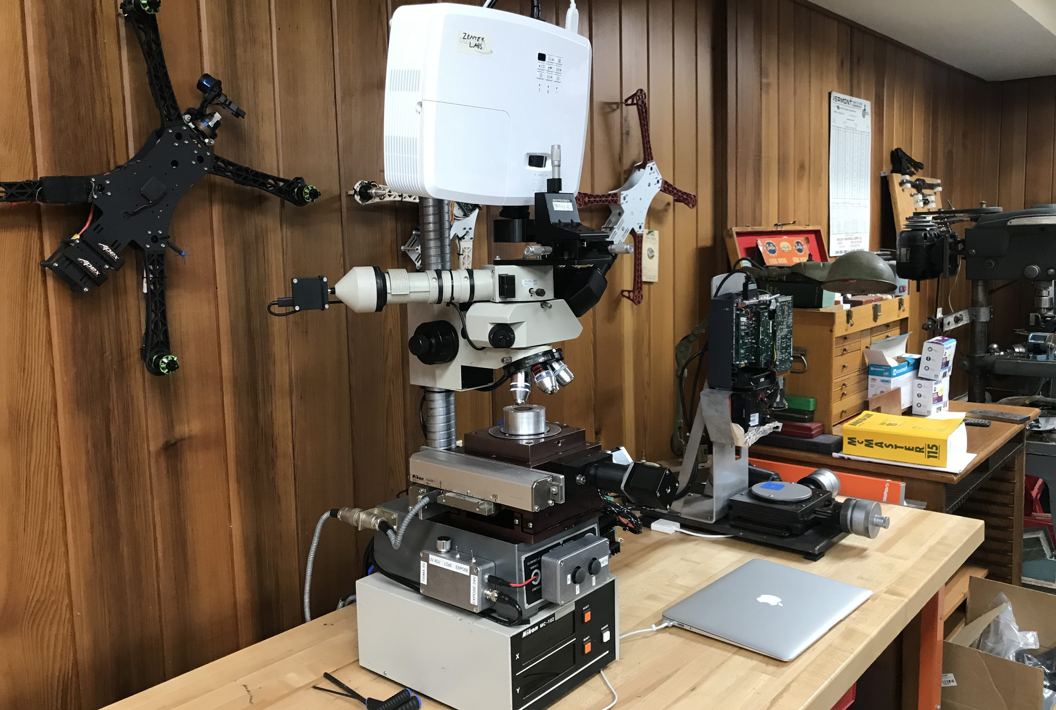
Geeze, I though you needed a clean room to do this kind of work. I guess, being a hobby, with less concern for effort, loss of product, or cost versus profit, one might summon the will to try, try again, when confronted with botched fabrication runs.
Even with millimeter-scale components, I'd still think dust and debris could be a real problem. Is it just that 12 hour runs are short enough to just accept an imperfect production output, since it's a personal project, or is dust not as big a deal at this scale as I'd imagine?
I was looking for how he managed the clean room or did he not go too small. Found the answer in the IEEE article shared by another commenter (he didn't go below 10 micron tech node).
But now I have a follow up question, if getting a clean room is obviously harder, isn't "clean box" more doable? E.g., if you line up a bunch of tables, and put a long box on top that acts like a poor man's assembly line. The insides of that box are only accessible through gloves that are attached to holes on the sides of the box, and plenty of glass windows to look inside (kinda like the box in movie 'Life'). How cost effective and feasible (i.e., gets the job done) would that be compared to a clean room? maybe you could go sub-micron with it if not sub-100nm.
Also if you don't really care about yield, many things are not that critical. I did a PhD in semi-conductor physics, and most processes for silicon are actually surprisingly robust (compared to processes of any other material). Also many things are just done the way because people know it worked before, which does not mean you can't use less fancy equipment and it would still work.
What I understand is while semiconductor machines live in clean rooms, the wafers never leave the hyper clean environment inside the machines. And when wafers move from machine to machine it's via sealed enclosures.
Using long plastic box with a 3 axis gantry inside might be doable.
You should really read "The Radioactive Boy Scout", about a teenager who attempts to build a nuclear reactor. The EPA ends up dismantling his shed in moon suits.
This is incredible work. I would have loved to have attempted this when I was in college. The field seemed so inaccessible, and now it makes me happy to see some homebrewer accomplishing things like this.
That's great! Are we anywhere near to making homebrew ICs on silicon at home? Yes, apparently we are! But it seems we are still far away from DIY kits, or even complete prototyping devices (like 3D printers).
At that scale his hacked together (amazingly cheap) optical lithography equipment will not serve. (See how well it did with 1um lines. That is the main problem.) Nor especially the photoresist process.
Chip printer that would make IC's that are better than what amateur can make from readily available cheap components on a PCB board would be used in the industry first.
There is small number of field-programmable analog array (FPAA) products and FPGA/FPAA hybrids in the market. I hope they become better and more available (never used one myself).
I think the chemicals would be the rub. HF is very nasty, as is 'piranha solution'. Both are extremely corrosive, obviously - so it would be hard to build a 'printer' that could deal with the handling and disposal.
Not to mention, a lot of the dopants are pretty nasty too.
Instead of using all these dangerous chemicals, can you use use an alternative like Ion Beam Etch (IBE) or some sort of plasma etching system (given that a person can build one and has the money for everything like turbopumps and grids)? Or is it mandatory to use something like HF to etch?
There are less dangerous ways to explore "building a CPU from scratch" that hit on the really interesting bits. "Digital Computer Electronics" by Malvino and Brown. You are given logic gates (and, or, nor, nand etc) and build up from there to a working CPU. The articles referenced about HF are terrifying. I am a programmer, but, have worked in a chemistry lap. Its just endless stinky stuff that will kill you in a variety of ways. The logic of how a CPU works is more interesting.
Just putting out next step learning challenges. I'm loving what he's doing, it's a great project, I hope he continues it by exploring different aspects of it.
Other challenges include smaller lithography and CMOS fabrication using a self-aligned gate process. But there are pitfalls ahead, including chemicals that can kill with in trace doses...
I fabricated my own ICs as a teen in my freshman year of college as part of our program, but that obviously wasn't at home. It was still awesome, just going through the entire process.
Can you do this in a garage? Absolutely, but learn everything you need to know from an ensemble of safety-minded mentors before you strike out on your own.
It's not just about safety for you, proper disposal of these chemicals is essential for the many generations to come. Sometimes it is inexpensive, sometimes it is costly. You need to know how before you start, or it costs a lot more.
(Also, you can get someone else to pay for the hardware, the infrastructure, the material, the resists, the reagents, the safety training, and the waste disposal if you work/volunteer at a university's photolithography facility. They'll probably pay you, too.)