Automotive grade, but allegedly still LPDDR4. Looks like they're x16 and x32, as you said.
--------
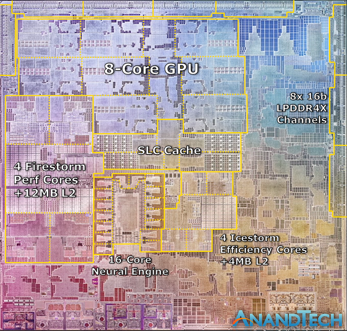
Hmmm, I know that the M1 is specified as 128-bits on Anandtech's site. If its 4-dies per chip, then 32-bits per die, 4-total dies of LPDDR4? I know Anandtech is claiming a 128-bit bus, so I'm reverse-engineering things from that tidbit of knowledge.
-----
Either way, these 128-bit or 64-bit numbers are all very much smaller than 1024-bit per stack HBM2 (high-bandwidth memory). Much, much, much much smaller. Its clear that the M1 isn't using HBM at all, but some kind of LPDDR4x configuration.
This chip claims to be LPDDR4x, but it is a 556-pin package. This is in contrast to your earlier data-sheet, which only has 200-pins. Maybe LPDDR4x doesn't have any standardized pinouts?
This isn't exactly where I normally work, so I'm not entirely sure what is going on.
I just went to Micron's page for LPDDR4: https://www.micron.com/products/dram/lpdram/automotive-lpddr...
Automotive grade, but allegedly still LPDDR4. Looks like they're x16 and x32, as you said.
--------
Hmmm, I know that the M1 is specified as 128-bits on Anandtech's site. If its 4-dies per chip, then 32-bits per die, 4-total dies of LPDDR4? I know Anandtech is claiming a 128-bit bus, so I'm reverse-engineering things from that tidbit of knowledge.
-----
Either way, these 128-bit or 64-bit numbers are all very much smaller than 1024-bit per stack HBM2 (high-bandwidth memory). Much, much, much much smaller. Its clear that the M1 isn't using HBM at all, but some kind of LPDDR4x configuration.