Of course. But it's been two years now. There are many civilians that would have such bugged motherboards, and they've had two years now to find out where the flaw is. Including civilian organizations that Bloomberg explicitly said were targeted.
That said, about this : Modified silicon or firmware would be very hard to detect.
This is not compatible with the mechanism Bloomberg is proposing. They are suggesting that some silicon in the motherboard is intercepting memory in real-time, processing it, and modifying it on-the-fly to make the CPU do what is wanted.
That is not something that can be done by merely modifying existing silicon. RAM is directly, physically connected to the CPU. You would need to add an extremely high performance chip that shouldn't be there between the CPU and the RAM, and there is simply no way to hide that.
Firmware attacks are possible, yes, but you can readout the content of firmware chips too.
It's not a mechanism of attack that could be done invisibly. At the easiest, you could detect it by a timing attack, at the worst you can just x-ray the board. But it cannot be invisible.
>That is not something that can be done by merely modifying existing silicon. RAM is directly, physically connected to the CPU. You would need to add an extremely high performance chip that shouldn't be there between the CPU and the RAM, and there is simply no way to hide that.
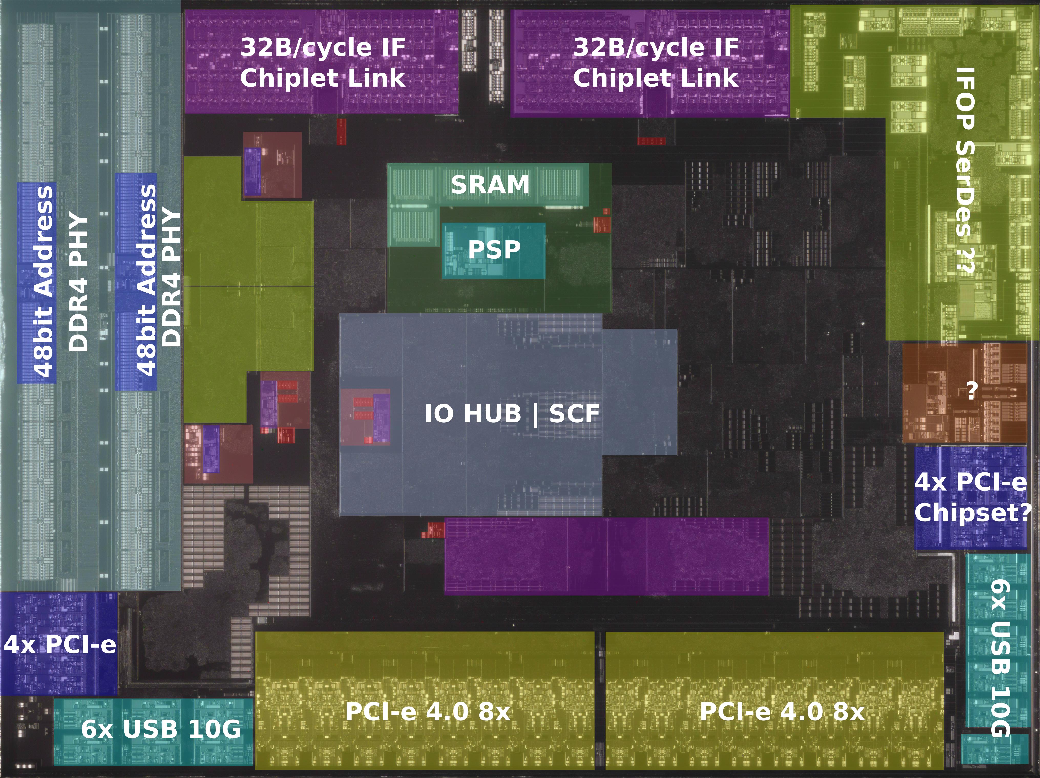
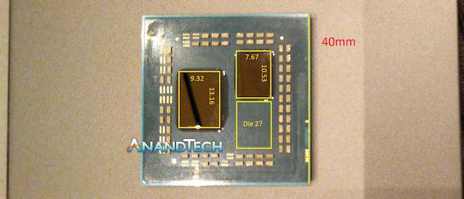
Why? Look at the die shot[1] of a zen 2 IO die (manufactured using 14 nm process), and see how small the DDR4 PHY blocks are in comparison to the rest of the chip. Then consider the whole picture only covers 9.3mm x 13.2mm. If you only cared about manipulating a few bits of the DDR4 data bus, I don't see why the package has to so large that you can't hide it. You could also go for the opposite approach (ie. rather than decoding the signal and injecting the correct signal, you introduce a glitch at the analog level, similar to how rowhammer works).
Look at a modern motherboard. See how thick the RAM bus is? On my X370 motherboard it's over 10 cm thick and goes down to around 3 cm thick as it goes through vias.
For your chip to interface, you'd have to reroute all those traces to it (because RAM is random access, you wouldn't have the context necessary to know when to inject or modify if you weren't accessing most of the traces).
On an X-ray of the motherboard, you'd see all those traces converge to a point, then diverge back onto the socket. On a normal motherboard x-ray[1], you see the traces make a trapezoidal pattern.
Such tampering would be immediately visible to a motherboard x-ray. And by the way, they would likely be detectable by software too, even just the delay introduced by the length of the traces is detectable.
In addition, you'd actually need to have the die also process the data from memory, and it would need to be quite a bit faster than the relatively slow Ryzen memory subsystem.


That said, about this : Modified silicon or firmware would be very hard to detect.
This is not compatible with the mechanism Bloomberg is proposing. They are suggesting that some silicon in the motherboard is intercepting memory in real-time, processing it, and modifying it on-the-fly to make the CPU do what is wanted.
That is not something that can be done by merely modifying existing silicon. RAM is directly, physically connected to the CPU. You would need to add an extremely high performance chip that shouldn't be there between the CPU and the RAM, and there is simply no way to hide that.
Firmware attacks are possible, yes, but you can readout the content of firmware chips too.
It's not a mechanism of attack that could be done invisibly. At the easiest, you could detect it by a timing attack, at the worst you can just x-ray the board. But it cannot be invisible.